


NONLINEAR OPTICAL CRYSTALS
PPLN Crystal -Periodically Poled Lithium Niobate
Periodically Poled Lithium Niobate (PPLN) crystal engineered for quasi-phase-matched wavelength conversion, high-efficiency nonlinear optics and customised frequency-conversion applications.
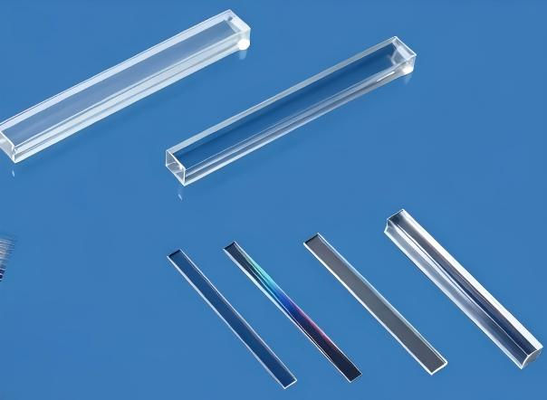
PPLN crystal material supplied by Yueneng Optoelectronics.
TECHNICAL DATA
PPLN Crystal Material & QPM Specifications
PPLN uses a periodically inverted domain structure to support quasi-phase matching, enabling efficient nonlinear wavelength conversion across a broad range of laser applications.
Type of Conversion
SHG / DFG / SFG / OPO / OPA / OPG
Grating Types
Single / Multi / Chirp / Fan-out / Cascade
QPM Period
Standard and customised, 4.0–200 μm
Transparency Range
330–5500 nm
Matching Temperature
25–200 °C
Thickness
Up to 5 mm
Length
Up to 55 mm
Duty Ratio
48–52% or customised
APPLICATIONS
High-Efficiency Wavelength Conversion
Frequency Doubling & Mixing
PPLN supports SHG, SFG and DFG configurations for efficient wavelength conversion using quasi-phase matching.
Optical Parametric Conversion
PPLN can be configured for OPO, OPA and OPG applications across specialised laser and photonics systems.
Custom Wavelength Conversion
Custom QPM periods and domain structures can be coordinated according to pump wavelength, target output wavelength and application requirements.
QPM ENGINEERING
PPLN Grating Configurations
PPLN domain structures can be configured for different wavelength-conversion requirements, supporting standard and customised quasi-phase-matching designs.

Single
Single-period grating configuration for defined wavelength-conversion conditions.
Multi
Multiple grating periods for different phase-matching conditions within one crystal design.
Cascade
Cascaded domain structures for multi-stage nonlinear conversion configurations.
Fan-out
Spatially varying grating periods enabling selection of different QPM conditions across the crystal aperture.
Chirp
Chirped grating structures with varying period along the interaction length.
DEVICE STRUCTURES
Bulk & Waveguide PPLN Structures
PPLN can be configured in different device structures according to pump laser power, conversion efficiency, output power and system size requirements.
PPLN device and domain structures can be customised according to specific optical system requirements.
Bulk
Buried Waveguide
Slab Waveguide
Ridge Waveguide
Integrated with Laser Crystal
Optically Contacted with Laser Crystal
PROCESSING CAPABILITY
Optical & Processing Specifications
PPLN crystals can be processed and configured according to wavelength-conversion and optical system requirements.
Flatness
λ/6 @ 632.8 nm
Parallelism
< 10 arc sec
Perpendicularity
< 10 arc min
Surface Quality
10-5
Crystal dimensions, QPM period, domain structure, coating and processing requirements can be discussed according to the application.

Coating Options
AR / HR
QPM Period
4.0–200 μm, standard or customised
Maximum Thickness
Up to 5 mm
Maximum Length
Up to 55 mm